Category: computers

Interesting pre-announced products that may or may not ship, and may or may not have an impact on desktop/network computing

  • ARM Pitches Tri-gate Transistors for 20nm and Beyond

    English: I am the author of this image.
    Image via Wikipedia

    . . . 20 nm may represent an inflection point in which it will be necessary to transition from a metal-oxide semiconductor field-effect transistor MOSFET to Fin-Shaped Field Effect Transistors FinFET or 3D transistors, which Intel refers to as tri-gate designs that are set to debut with the companys 22 nm Ivy Bridge product generation.

    via ARM Pitches Tri-gate Transistors for 20nm and Beyond.

    Three Dimensional transistors in the news again. Previously Intel announced they were adopting a new design for their next generation next smaller design rule for the Ivy Bridge generation Intel CPUs. Now ARM is also doing work to integrate similar technology into their ARM cpu cores as well. No doubt in order to lower Thermal Design Point and maintain clock speed as well are both driving this move to refine and narrow the design rules for the ARM architecture. Knowing Intel is still the top research and development outfit for silicon semi-conductors would give pause to anyone directly competing with them, but ARM is king of the low power semi-conductor and keeping pace with Intel’s design rules is an absolute necessity.

    I don’t know how quickly ARM is going to be able to get a licensee to jump onboard and adopt the new design. Hopefully a large operation like Samsung can take this on and get the chip into it’s design, development, production lines at a chip fabrication facility as soon as possible. Likewise other contract manufacturers like Taiwan Semiconductor Manufacturing Company (TSMC) should also try to get this chip into their facilities quickly too. That way the cell-phone and tablet markets can benefit too as they use a lot of ARM licensed cpu cores and similar intellectual property in their shipping products. And my interest is not so much invested in the competition between Intel and ARM for low power computing but more the overall performance of any single ARM design once it’s been in production for a while and optimized the way Apple designs its custom CPUs using ARM licensed cpu cores. The single most outstanding achievement of Apple in their design and production of the iPad is the battery charge duration of 10 hours. Which to date, is an achievement that has not been beaten, even by other manufacturers and products who also license ARM intellectual property. So if  the ARM design is good and can be validated and proto-typed with useful yields quickly, Apple will no doubt be the first to benefit, and by way of Apple so will the consumer (hopefully).

    Schematic view (L) and SEM view (R) of Intel t...
    Image via Wikipedia
  • Tilera | Wired Enterprise | Wired.com

    Tilera’s roadmap calls for its next generation of processors, code-named Stratton, to be released in 2013. The product line will expand the number of processors in both directions, down to as few as four and up to as many as 200 cores. The company is going from a 40-nm to a 28-nm process, meaning they’re able to cram more circuits in a given area. The chip will have improvements to interfaces, memory, I/O and instruction set, and will have more cache memory.

    via Tilera | Wired Enterprise | Wired.com.

    Image representing Wired Magazine as depicted ...
    Image via CrunchBase

    I’m enjoying the survey of companies doing massively parallel, low power computing products. Wired.com|Enterprise started last week with a look at SeaMicro and how the two principal founders got their start observing Google’s initial stabs at a warehouse sized computer. Since that time things have fractured somewhat instead of coalescing and now three big attempts are competing to fulfil the low power, massively parallel computer in a box. Tilera is a longer term project startup from MIT going back further than Calxeda or SeaMicro.

    However application of this technology has been completely dependent on the software. Whether it be OSes or Applications, they all have to be constructed carefully to take full advantage of the Tile processor architecture. To their credit Tilera has attempted to insulate application developers from some of the vagaries of the underlying chip by creating an OS that does the heavy lifting of queuing and scheduling. But still, there’s got to be a learning curve there even if it isn’t quite as daunting as say folks who develop applications for the super computers at National Labs here in the U.S. Suffice it to say it’s a non-trivial choice to adopt a Tilera cpu for a product/project you are working on. And the people who need a Tilera GX cpu for their app, already know all they need to know about the the chip in advance. It’s that kind of choice they are making.

    I’m also relieved to know they are continuing development to shrink down the design rules. Intel being the biggest leader in silicon semi-conductor manufacturing, continues to shrink its design, development and manufacturing design rules. We’re fast approaching a 20nm-18nm production line in both Oregon and Arizona. Both are Intel design fabrication plants and there not about to stop and take a breath. Companies like Tilera, Calxeda and SeaMicro need to do continuous development on their products to keep from being blind sided by Intel’s continuous product development juggernaut. So Tilera is very wise to shrink its design rule from 40nm down to 28nm as fast as it can and then get good yields on the production lines once they start sampling chips at this size.

    *UPDATE: Just saw this run through my blogroll last week. Tilera has announced a new chip coming in March. Glad to see Tilera is still duking it out, battling for the design wins with manufacturers selling into the Data Center as it were. Larger Memory addressing will help make the Tilera chips more competitive with Commodity Intel Hardware shops, and maybe we’ll see full 64bit memory extensions at some point as a follow on to the current 40bit address space extenstions currently being touted in this article from The Register.

    English: Block diagram of the Tilera TILEPro64...
    Image via Wikipedia
  • How Google Spawned The 384-Chip Server | Wired Enterprise | Wired.com

    SeaMicro’s latest server includes 384 Intel Atom chips, and each chip has two “cores,” which are essentially processors unto themselves. This means the machine can handle 768 tasks at once, and if you’re running software suited to this massively parallel setup, you can indeed save power and space.

    via How Google Spawned The 384-Chip Server | Wired Enterprise | Wired.com.

    Image representing Wired Magazine as depicted ...
    Image via CrunchBase

    Great article from Wired.com on SeaMicro and the two principle minds behind its formation. Both of these fellows were quite impressed with Google’s data center infrastructure at the points in time when they both got to visit a Google Data Center. But rather than just sit back and gawk, they decided to take action and borrow, nay steal some of those interesting ideas the Google Engineers adopted early on. However, the typical naysayers pull a page out of the Google white paper arguing against SeaMicro and the large number of smaller, lower-powered cores they use in the SM-10000 product.

    SeaMicro SM10000
    Image by blogeee.net via Flickr

    But nothing speaks of success more than product sales and SeaMicro is selling it’s product into data centers. While they may not achieve the level of commerce reached by Apple Inc., it’s a good start. What still needs to be done is more benchmarks and real world comparisons that reproduce or negate the results of Google’s whitepaper promoting their choice of off the shelf commodity Intel chips. Google is adamant that higher clock speed ‘server’ chips attached to single motherboards connected to one another in large quantity is the best way to go. However, the two guys who started SeaMicro insist that while Google’s choice for itself makes perfect sense, NO ONE else is quite like Google in their compute infrastructure requirements. Nobody has such a large enterprise or the scale Google requires (except for maybe Facebook, and possibly Amazon). So maybe there is a market at the middle and lower end of the data center owner’s market? Every data center’s needs will be different especially when it comes to available space, available power and cooling restrictions for a given application. And SeaMicro might be the secret weapon for shops constrained by all three: power/cooling/space.

    *UPDATE: Just saw this flash through my Google Reader blogroll this past Wednesday, Seamicro is now selling an Intel Xeon based server. I guess the market for larger numbers of lower power chips just isn’t strong enough to sustain a business. Sadly this makes all the wonder and speculation surrounding the SM10000 seem kinda moot now. But hopefully there’s enough intellectual property rights and patents in the original design to keep the idea going for a while. Seamicro does have quite a headstart over competitors like Tilera, Calxeda and Applied Micro. And if they can help finance further developments of Atom based servers by selling a few Xeons along the way, all the better.

  • RE: Erics Archived Thoughts: Vigilance and Victory

    Erics Archived Thoughts: Vigilance and Victory.

    While I agree there might be a better technical solution to the DNS blocking adopted by SOPA and PIPA bills, less formal networks are in essence filling the gap. By this I mean the MegaUpload takedown that occurred yesterday at the the order of the U.S. Justice Department. Without even the benefit of SOPA or PIPA, they ordered investigations, arrests and takedowns of the whole MegaUpload enterprise. But what is interesting is the knock-on effects social networks had in the vacuum left by the DNS blocking. Within hours the DNS was replaced by it’s immediate pre-cursors. That’s right, folks were sending the IP addresses of available MegaUpload hosts by plain text in Tweet messages the world ’round. And given the announcement today that Twitter will be closing in on it’s 500 Million’th account being created I’m not too worried about a technical solution to DNS blocking. That too is already moot, by virtue of the the fact of social networking and simple numeric IP addresses. Long live IPv4 and the quadruple octets 255.255.255.xxx

  • AnandTech – AMD Radeon HD 7970 Review: 28nm And Graphics Core Next, Together As One

    Image representing AMD as depicted in CrunchBase
    Image via CrunchBase

    Quick Sync made real-time H.264 encoding practical on even low-power devices, and made GPU encoding redundant at the time. AMD of course isn’t one to sit idle, and they have been hard at work at their own implementation of that technology: the Video Codec Engine VCE.

    via AnandTech – AMD Radeon HD 7970 Review: 28nm And Graphics Core Next, Together As One.

    Intel’s QuickSync helped speed up the realtime encoding of H.264 video. AMD is striking back and has Hybrid Mode VCE operations that will speed things up EVEN MORE! The key to having this hit the market and get widely adopted of course is the compatibility of the software with a wide range of video cards from AMD. The original CUDA software environment from nVidia took a while to disperse into the mainstream as it had a limited number of graphics cards it could support when it rolled out. Now it’s part of the infrastructure and more or less provided gratis whenever you buy ANY nVidia graphics card today. AMD has to follow this semi-forced adoption of this technology as fast as possible to deliver the benefit quickly. At the same time the User Interface to this VCE software had better be a great design and easy to use. Any type of configuration file dependencies and tweaking through preference files should be eliminated to the point where you merely move a slider up and down a scale (Slower->Faster). And that should be it.

    And if need be AMD should commission an encoder App or a plug-in to an open source project like HandBrake to utilize the VCE capability upon detection of the graphics chip on the computer. Make it ‘just happen’ without the tempting early adopter approach of making a tool available and forcing people to ‘build’ a version of an open source encoder to utilize the hardware properly. Hands-off approaches that favor early adopters is going to consign this technology to the margins for a number of years if AMD doesn’t take a more activist role. QuickSync on Intel hasn’t been widely touted either so maybe it’s a moot point to urge anyone to treat their technology as an insanely great offering. But I think there’s definitely brand loyalty that could be brought into play if the performance gains to be had with a discreet graphics card far outpace the integrated graphics solution of QuickSync provided by Intel. If you can achieve a 10x order of magnitude boost, you should be pushing that to all the the potential computer purchasers from this announcement forward.

  • Maxeler Makes Waves With Dataflow Design – Digits – WSJ

    In the dataflow approach, the chip or computer is essentially tailored for a particular program, and works a bit like a factory floor.

    via Maxeler Makes Waves With Dataflow Design – Digits – WSJ.

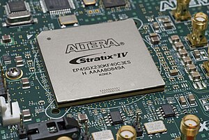
    English: Altera Stratix IV EP4SGX230 FPGA on a PCB
    Image via Wikipedia

    My supercomputer can beat your supercomputer, and money is no object. FPGAs (Field Programmable Gate Arrays) are used most often in prototyping new computer processors. You can design a chip, then ‘program’ the FPGA to match the circuit design so that it can be verified. Verification is the process by which you do exhaustive tests on the logic and circuits to see if you’ve left anything out or didn’t get the timing right for the circuits that may run at different speeds within the chip itself. They are expensive niche products that chip design outfits and occasionally product manufacturers use to solve problems. Less often they might be used in data network gear to help classify and reroute packets in a data center and optimize performance over time.

    This by itself would be a pretty good roster of applications, but something near and dear to my heart is the use of FPGAs as a kind of reconfigurable processor. I am certain one day we will see the application of FPGA  in desktop computers. But until then, we’ll have to settle for using FPGAs as special purpose application accelerators in high volume trading and Wall Street type data centers. This article in WSJ is going to change a few opinions about the application of FPGAs for real computing tasks. The speedups quoted for different analysis and reports derived from the transactions show multiple orders of magnitude speedups. In extreme examples sometimes 1,000 times faster speed-ups occurred when using a fully optimized FPGA versus a general purpose CPU.

    When someone can tout 1,000X speedups everyone is going to take notice. And hopefully it won’t be simply a bunch of copycats trying to speed up their reports and management dashboards. There’s a renaissance out there waiting to happen with FPGAs and I still have hope I’ll see it in my lifetime.

  • Xen hypervisor ported to ARM chips • The Register

    Deutsch: Offizielles Logo der ARM-Prozessorarc...
    Image via Wikipedia

    You can bet that if ARM servers suddenly look like they will be taking off that Red Hat and Canonical will kick in some help and move these Xen and KVM projects along. Server maker HP, which has launched the “Redstone” experimental server line using Calxedas new quad-core EnergyCore ARM chips, might also help out. Dell has been playing around with ARM servers, too, and might help with the hypervisor efforts as well.

    via Xen hypervisor ported to ARM chips • The Register.

    This is an interesting note, some open source Hypervisor projects are popping up now that the ARM Cortex A15 has been announced and some manufacturers are doling out development boards. What it means longer term is hard to say other than it will potentially be a boon to manufacturers using the ARM15 in massively parallel boxes like Calxeda. Or who are trying to ‘roll their own’ ARM based server farms and want to have the flexibility of virtual machines running under a hypervisor environment. However, the argument remains, “Why use virtual servers on massively parallel cpu architectures when a  1:1 cpu core to app ratio is more often preferred?”

    However, I would say old habits of application and hardware consolidation die hard and virtualization is going to be expected because that’s what ‘everyone’ does in their data centers these days. So knowing that a hypervisor is available will help foster some more hardware sales of what will most likely be a niche products for very specific workloads (ie. Calxeda, Qanta SM-2, SeaMicro). And who knows maybe this will foster more manufacturers or even giant data center owners (like Apple, Facebook and Google) to attempt experiments of rolling their own ARM15 environments knowing there’s a ready made hypervisor out there that they can compile on the new ARM chip.

    However, I think all eyes are really still going to be on the next generation ARM version 8 with the full 64bit memory and instruction set. Toolsets nowadays are developed in house by a lot of the datacenters and the dominant instruction set is Intel x64 (IA64) which means the migration to 64bits has already happened. Going back to 32bits just to gain the advantage of the lower power ARM architecture is far to costly for most. Whereas porting from IA64 to 64bit ARM architecture is something more datacenters might be willing to do if the potential cost/benefit ratio is high enough to cross-compile and debug. So legacy management software toolsets are really going to drive a lot of testing and adoption decisions by data centers looking at their workloads and seeing if ARM cpus fit their longer term goals of saving money by using less power.

  • Disruptions: Wearing Your Computer on Your Sleeve – NYTimes.com

    English: This depicts the evolution of wearabl...
    Image via Wikipedia: Bad old days of Wearable Computers

    Wearable computing is a broad term. Technically, a fancy electronic watch is a wearable computer. But the ultimate version of this technology is a screen that would somehow augment our vision with information and media.

    via Disruptions: Wearing Your Computer on Your Sleeve – NYTimes.com.

    Augmented Reality in the news, only this time it’s Google so it’s like for rilz, yo! Just kidding, it will be very interesting given Google’s investment in the Android OS and power-saving mobile computing what kind of wearable computers they will develop. No offense to MIT Media Lab, but getting something into the hands of end-users is something Google is much more accomplished at doing (but One Laptop Per Child however is the counter-argument of course). I think mobile phones are already kind of like a wearable computer. Think back to the first iPod arm bands right? Essentially now just scale the ipod up to the size of an Android and it’s no different. It’s practically wearable today (as Bilton says in his article).

    What’s different then with this effort is the accessorizing of the real wearable computer (the smart phone) giving it the augmentation role we’ve seen with products like Layar. But maybe not just limited to cameras, video screens and information overlays, the next wave would have auxiliary wearable sensors communicating back to the smartphone like the old Nike accelerometer that would fit into special Nike Shoes. And also consider the iPod Nano ‘wrist watch’ fad as it exists today. It may not run the Apple iOS, but it certainly could transmit data to your smartphone if need be. Which leads to the hints and rumors of attempts by Apple to create ‘curved glass’.

    This has been an ongoing effort by Apple, without being tied to any product or feature in their current product line. Except maybe the iPhone. Most websites I’ve read to date speculate the curvature is not very pronounced and a styling cue to further help marketing and sales of the iPhone. But in this article the curvature Bilton is talking about would be more like the face of a bracelet around the wrist, much more pronounced. Thus the emphasis on curved glass might point to more work being done on wearable computers.

    Lastly Bilton’s article goes into a typical futuristic projection of what form the video display will take. No news to report on this topic specifically as it’s a lot of hand-waving and make believe where contact lenses potentially can become display screens. As for me, the more pragmatic approach of companies like Layar creating iPhone/Augmented Reality software hybrids is going to ship sooner and prototype faster than the make believe video contact lenses of the Future.The takeaway I get from Bilton’s article is there’s more of a defined move to create more functions with the smartphone as more of a computer. Though MIT Media Lab have labeled this ‘wearable computing’ think of it more generally as Ubiquitous Computing where the smartphone and its data connection are with you wherever you go.

  • The PC is dead. Why no angry nerds? :: The Future of the Internet — And How to Stop It

    Famously proprietary Microsoft never dared to extract a tax on every piece of software written by others for Windows—perhaps because, in the absence of consistent Internet access in the 1990s through which to manage purchases and licenses, there’d be no realistic way to make it happen.

    via The PC is dead. Why no angry nerds? :: The Future of the Internet — And How to Stop It.

    While true that Microsoft didn’t tax Software Developers who sold product running on the Windows OS, a kind of a tax levy did exist for hardware manufacturers creating desktop pc’s with Intel chips inside. But message received I get the bigger point, cul-de-sacs don’t make good computers. They do however make good appliances. But as the author Jonathan Zittrain points out we are becoming less aware of the distinction between a computer and an applicance, and have lowered our expectation accordingly.

    In fact this points to the bigger trend of not just computers becoming silos of information/entertainment consumption no, not by a long shot. This trend was preceded by the wild popularity of MySpace, followed quickly by Facebook and now Twitter. All platforms as described by their owners with some amount of API publishing and hooks allowed to let in 3rd party developers (like game maker Zynga). But so what if I can play Scrabble or Farmville with my ‘friends’ on a social networking ‘platform’? Am I still getting access to the Internet? Probably not, as you are most likely reading what ever filters into or out of the central all-encompassing data store of the Social Networking Platform.

    Like the old World Maps in the days before Columbus, there be Dragons and the world ends HERE even though platform owners might say otherwise. It is an Intranet pure and simple, a gated community that forces unique identities on all participants. Worse yet it is a big brother-like panopticon where each step and every little movement monitored and tallied. You take quizzes, you like, you share, all these things are collection points, check points to get more data about you. And that is the TAX levied on anyone who voluntarily participates in a social networking platform.

    So long live the Internet, even though it’s frontier, wild-catting days are nearly over. There will be books and movies like How the Cyberspace was Won, and the pioneers will all be noted and revered. We’ll remember when we could go anywhere we wanted and do lots of things we never dreamed. But those days are slipping as new laws get passed under very suspicious pretenses all in the name of Commerce. As for me I much prefer Freedom over Commerce, and you can log that in your stupid little database.

    Cover of "The Future of the Internet--And...
    Cover via Amazon
  • AnandTech – Applied Micros X-Gene: The First ARMv8 SoC

    APM expects that even with a late 2012 launch it will have a 1 – 2 year lead on the competition. If it can get the X-Gene out on time, hitting power and clock targets both very difficult goals, the headstart will be tangible. Note that by the end of 2012 well only just begin to see the first Cortex A15 implementations. ARMv8 based competitors will likey be a full year out, at least. 

    via AnandTech – Applied Micros X-Gene: The First ARMv8 SoC.

    Chip Diagram for the ARM version 8 as implemented by APM

    It’s nice to get a confirmation of the production time lines for the Cortex A15 and the next generation ARM version 8 architecture. So don’t expect to see shipping chips, much less finished product using those chips well into 2013 or even later. As for the 4 core ARM A15, finished product will not appear until well into 2012. This means if Intel is able to scramble, they have time to further refine their Atom chips to reach the power level and Thermal Design Point (TDP) for the competing ARM version 8 architecture. What seems to be the goal is to jam in more cores per CPU socket than is currently done on the Intel architecture (up to almost 32 in on of the graphics presented with the article).

    The target we are talking about is 2W per core @ 3Ghz, and it is going to be a hard, hard target to hit for any chip designer or manufacturer. One can only hope that TMSC can help APM get a finished chip out the door on it’s finest ruling chip production lines (although an update to the article indicates it will ship on 40nm to get it out the door quicker). The finer the ruling of signal lines on the chip the lower the TDP, and the higher they can run the clock rate. If ARM version 8 can accomplish their goal of 2W per cpu core @ 3 Gigahertz, I think everyone will be astounded. And if this same chip can be sampled at the earliest prototypes stages by a current ARM Server manufacturer say, like Calxeda or even SeaMicro then hopefully we can get benchmarks to show what kind of performance can be expected from the ARM v.8  architecture and instruction set. These will be interesting times.

    Intel Atom CPU Z520, 1,333GHz
    Image via Wikipedia