Category: data center

  • Fusion-io shoves OS aside, lets apps drill straight into flash • The Register

    Like the native API libraries, directFS is implemented directly on ioMemory, significantly reducing latency by entirely bypassing operating system buffer caches, file system and kernel block I/O layers. Fusion-io directFS will be released as a practical working example of an application running natively on flash to help developers explore the use of Fusion-io APIs.

    via (Chris Mellor) Fusion-io shoves OS aside, lets apps drill straight into flash • The Register.

    Image representing Fusion-io as depicted in Cr...
    Image via CrunchBase

    Another interesting announcement from the folks at Fusion-io regarding their brand of PCIe SSD cards. There was a proof of concept project covered previously by Chris Mellor in which Fusion-io attempted to top out at 1 Billion IOPs using a novel architecture where PCIe SSD drives were not treated as storage. In fact the Fusion-io was turned into a memory tier bypassing most of the OSes own buffers and queues for handling a traditional Filesystem. Doing this reaped many benefits in terms of depleting the latency inherent with a FileSystem and how it has to communicate through the OS kernel through to the memory subsystem and back again.

    Considering also work done within the last 4 years or more using so-called “in memory’ databases and big data projects in general a product like directFS might pair nicely with them. The limit with in memory databases is always the amount of RAM available and total number of cpu nodes managing those memory subsystems. Tack on the necessary storage to load and snapshot the database over time and you have a very traditional looking database server. However, if you supplement that traditional looking architecture with a tier of storage like the directFS the SAN network becomes a 3rd tier of storage, almost like a tape backup device. Sounds interesting the more I daydream about it.

    Shows the kernel's role in a computer.
    Shows the kernel’s role in a computer. (Photo credit: Wikipedia)
  • AMD Snatches New-Age Server Maker From Under Intel | Wired Enterprise | Wired.com

    Image representing AMD as depicted in CrunchBase
    Image via CrunchBase

    Chip designer and chief Intel rival AMD has signed an agreement to acquire SeaMicro, a Silicon Valley startup that seeks to save power and space by building servers from hundreds of low-power processors.

    via AMD Snatches New-Age Server Maker From Under Intel | Wired Enterprise | Wired.com.

    It was bound to happen eventually, I guess. SeaMicro has been acquired by AMD. We’ll see what happens as a result as SeaMicro is a customer of Intel’s Atom chips and now most recently Xeon server chips as well. I have no idea where this is going or what AMD intends to do, but hopefully this won’t scare off any current or near future customers.

    SeaMicro’s competitive advantage has been and will continue to be the development work they performed on that custom ASIC chip they use in all their systems. That bit of intellectual property was in essence the reason AMD decided to acquire SeaMicro and hopefully let it gain an engineering advantage for systems it might put out on the market in the future for large scale Data Centers.

    While this is all pretty cool technology, I think that SeaMicro’s best move was to design its ASIC so that it could take virtually any common CPU. In fact, SeaMicro’s last big announcement introduced its SM10000-EX option, which uses low-power, quad-core Xeon processors to more than double compute performance while still keeping the high density, low-power characteristics of its siblings.

    via SeaMicro acquisition: A game-changer for AMD • The Register.

    So there you have it Wired and The Register are reporting the whole transaction pretty positively. Looks on the surface to be a win for AMD as it can design new server products and get them to market quickly using the SeaMicro ASIC as a key ingredient. SeaMicro can still service it’s current customers and eventually allow AMD to up sell or upgrade as needed to keep the ball rolling. And with AMD’s Fusion architecture marrying GPUs with CPU cores who knows what cool new servers might be possible? But as usual the nay-sayers the spreaders of Fear, Uncertainty and Doubt have questioned the value of SeaMicro and their original product he SM-10000.

    Diane Bryant, the general manager of Intel’s data center and connected systems group at a press conference for the launch of new Xeon processors had this to say, ““We looked at the fabric and we told them thereafter that we weren’t even interested in the fabric,” when asked about SeaMicro’s attempt to interest Intel in buying out the company. To Intel there’s nothing special enough in the SeaMicro to warrant buying the company. Furthermore Bryant told Wired.com:

    “…Intel has its own fabric plans. It just isn’t ready to talk about them yet. “We believe we have a compelling solution; we believe we have a great road map,” she said. “We just didn’t feel that the solution that SeaMicro was offering was superior.”

    This is a move straight out of Microsoft’s marketing department circa 1992 where they would pre-announce a product that never shipped was barely developed beyond a prototype stage. If Intel is really working on this as a new product offering you would have seen an announcement by now, rather than a vague, tangential reference that appears more like a parting shot than a strategic direction. So I will be watching intently in the coming months and years if needed to see what if any Intel ‘fabric technology’ makes its way from the research lab, to the development lab and to final product shipping. However don’t be surprised if this is Intel attempting to undermine AMD’s choice to purchase SeaMicro. Likewise, Forbes.com later reported from a representative from SeaMicro that their company had not tried to encourage Intel to acquire SeaMicro. It is anyone’s guess who is really correct and being 100% honest in their recollections. However I am still betting on SeaMicro’s long term strategy of pursuing low power, ultra dense, massively parallel servers. It is an idea whose time has come.

    Image representing Intel as depicted in CrunchBase
    Image via CrunchBase
  • Facebook Shakes Hardware World With Own Storage Gear | Wired Enterprise | Wired.com

    Image representing Facebook as depicted in Cru...
    Image via CrunchBase

    Now, Facebook has provided a new option for these big name Wall Street outfits. But Krey also says that even among traditional companies who can probably benefit from this new breed of hardware, the project isn’t always met with open arms. “These guys have done things the same way for a long time,” he tells Wired.

    via Facebook Shakes Hardware World With Own Storage Gear | Wired Enterprise | Wired.com.

    Interesting article further telling the story of Facebook’s Open Compute project. This part of the story concentrates on the mass storage needs of the social media company. Which means Wall Street data center designer/builders aren’t as enthusiastic about Open Compute as one might think. The old school Wall Streeters have been doing things the same way as Peter Krey says for a very long time. But that gets to the heart of the issue, what the members of the Open Compute project hope to accomplish. Rack Space AND Goldman Sachs are members, both contributing and getting pointers from one another. Rack Space is even beginning to virtualize equipment down to the functional level replacing motherboards with a Virtual I/O service. That would allow components to be ganged up together based on the frequency of their replacement and maintenance. According to the article, CPUs could be in one rack cabinet, DRAM in another, Disks in yet another (which is already the case now with storage area networks).

    The newest item to come into the Open Compute circus tent is storage. Up until now that’s been left to Value Added Resellers (VARs) to provide. So different brand loyalties and technologies still hold sway for many Data Center shops including Open Compute. Now Facebook is redesigning the disk storage rack to create a totally tool-less design. No screws, no drive carriers, just a drive and a latch and that is it. I looked further into this tool-less phenomenon and found an interesting video at HP

    HP Z-1 all in one CAD workstation

    Along with this professional video touting how easy it is to upgrade this all in one design:

    The Making of the HP Z1

    Having recently purchased a similarly sized iMac 27″ and upgrading it by adding a single SSD drive into the case, I can tell you this HP Z1 demonstrates in every way possible the miracle of toolless designs. I was bowled over and remember back to some of my memories of different Dell tower designs over the years (some with more toolless awareness than others). If a toolless future is inevitable I say bring it on. And if Facebook ushers in the era of toolless Storage Racks as a central design tenet of Open Compute so much the better.

    Image representing Goldman Sachs as depicted i...
    Image via CrunchBase
  • SeaMicro adds Xeons to Atom smasher microservers • The Register

    Theres some interesting future possibilities for the SeaMicro machines. First, SeaMicro could extend that torus interconnect to span multiple chassis. Second, it could put a “Patsburg” C600 chipset on an auxiliary card and actually make fatter SMP nodes out of single processor cards and then link them into the torus interconnect. Finally, it could of course add other processors to the boards, such as Tileras 64-bit Tile Gx3000s or 64-bit ARM processors when they become available.

    via SeaMicro adds Xeons to Atom smasher microservers • The Register.

    SeaMicro SM10000
    SeaMicro SM10000 (Photo credit: blogeee.net)

    Timothy Prickett Morgan writing for The Register, has a great article on SeaMicro’s recent announcement of a Xeon-based 10U server chassis. Seemingly going against it’s first two generations of low power massively parallel server boxes, this one uses a brawny Intel Xeon server chip (albeit one that is fairly low power and low Thermal Design Point).

    Sad as it may seem to me, the popularity of the low power, massively parallel cpu box must not be very lucrative. But a true testament to the flexibility of their original 10U server rack design is the ability to do a ‘swap’ of the higher power Intel Xeon cpus. I doubt there’s too many competitors in this section of the market that could ‘turn on a dime’ the way SeaMicro has appeared to do with this Xeon based server. Most often designs will be so heavily optimized for a particular cpu, power supply and form factor layout that changing one component might force a bigger change order in the design department. And the product would take longer to develop and ship as a result.

    So even though I hope the 64bit Intel Atom will still be SeaMicro’s flagship product, I’m also glad they can stay in the fight longer selling into the ‘established’ older data center accounts worldwide. Adapt or die is the cliche adage of some technology writers and I would mark this with a plus (+) in the adapt column.

  • Tilera preps many-cored Gx chips for March launch • The Register

    “Were here today shipping a 64-bit processor core and we are what looks like two years ahead of ARM,” says Bishara. “The architecture of the Tile-Gx is aligned to the workload and gives one server node per chip rather than a sea of wimpy nodes not acting in a cache coherent manner. We have been in this market for two years now and we know what hurts in data centers and what works. And 32-bit ARM just is not going to cut it. Applied Micro is doing their own core, and that adds a lot of risks.”

    via Tilera preps many-cored Gx chips for March launch • The Register.

    Tile of a TILE64 processor from Tilera
    Image via Wikipedia

    Tilera is preparing to ship a 36 core Tile-Gx cpu in March. It’s going to be packaged with a re-compiled Linux distribution of CentOS on a development board (TILEencore). It will also have a number of re-compiled Unix utilities and packages included, so OEM shops can begin product development as soon as possible.

    I’m glad to see Tilera is still duking it out, battling for the design wins with manufacturers selling into the Data Center as it were. Larger Memory addressing will help make the Tilera chips more competitive with Commodity Intel Hardware data center shops who build their own hardware. Maybe we’ll see full 64bit memory extensions at some point as a follow on to the current 40bit address space extensions currently. The memory extensions are necessary to address more than the 32bit limit of 4GBytes, so an extra 8 bits goes a long, long way to competing against a fully 64bit address space.

    Also considering work being done at ARM for optimizing their chip designs for narrower design rules, Tilera should follow suit and attempt to shrink their chip architecture too. This would allow clock speeds to ease upward and keep the thermal design point consistent with previous generation Tile architecture chips, making Tile-Gx more competitive in the coming years. ARM announced 1 month ago they will be developing a 22nm sized cpu core for future licensing by ARM customers. As it is now Tilera uses an older fabrication design rule of around 40nm (which is still quite good given the expense required to shrink to lower design rules). And they have plans to eventually migrate to a narrower design rule. However ideally they would not stay farther behind that 1 generation from the top-end process lines of Intel (who is targeting 14nm production lines in the near future).

  • Tilera | Wired Enterprise | Wired.com

    Tilera’s roadmap calls for its next generation of processors, code-named Stratton, to be released in 2013. The product line will expand the number of processors in both directions, down to as few as four and up to as many as 200 cores. The company is going from a 40-nm to a 28-nm process, meaning they’re able to cram more circuits in a given area. The chip will have improvements to interfaces, memory, I/O and instruction set, and will have more cache memory.

    via Tilera | Wired Enterprise | Wired.com.

    Image representing Wired Magazine as depicted ...
    Image via CrunchBase

    I’m enjoying the survey of companies doing massively parallel, low power computing products. Wired.com|Enterprise started last week with a look at SeaMicro and how the two principal founders got their start observing Google’s initial stabs at a warehouse sized computer. Since that time things have fractured somewhat instead of coalescing and now three big attempts are competing to fulfil the low power, massively parallel computer in a box. Tilera is a longer term project startup from MIT going back further than Calxeda or SeaMicro.

    However application of this technology has been completely dependent on the software. Whether it be OSes or Applications, they all have to be constructed carefully to take full advantage of the Tile processor architecture. To their credit Tilera has attempted to insulate application developers from some of the vagaries of the underlying chip by creating an OS that does the heavy lifting of queuing and scheduling. But still, there’s got to be a learning curve there even if it isn’t quite as daunting as say folks who develop applications for the super computers at National Labs here in the U.S. Suffice it to say it’s a non-trivial choice to adopt a Tilera cpu for a product/project you are working on. And the people who need a Tilera GX cpu for their app, already know all they need to know about the the chip in advance. It’s that kind of choice they are making.

    I’m also relieved to know they are continuing development to shrink down the design rules. Intel being the biggest leader in silicon semi-conductor manufacturing, continues to shrink its design, development and manufacturing design rules. We’re fast approaching a 20nm-18nm production line in both Oregon and Arizona. Both are Intel design fabrication plants and there not about to stop and take a breath. Companies like Tilera, Calxeda and SeaMicro need to do continuous development on their products to keep from being blind sided by Intel’s continuous product development juggernaut. So Tilera is very wise to shrink its design rule from 40nm down to 28nm as fast as it can and then get good yields on the production lines once they start sampling chips at this size.

    *UPDATE: Just saw this run through my blogroll last week. Tilera has announced a new chip coming in March. Glad to see Tilera is still duking it out, battling for the design wins with manufacturers selling into the Data Center as it were. Larger Memory addressing will help make the Tilera chips more competitive with Commodity Intel Hardware shops, and maybe we’ll see full 64bit memory extensions at some point as a follow on to the current 40bit address space extenstions currently being touted in this article from The Register.

    English: Block diagram of the Tilera TILEPro64...
    Image via Wikipedia
  • How Google Spawned The 384-Chip Server | Wired Enterprise | Wired.com

    SeaMicro’s latest server includes 384 Intel Atom chips, and each chip has two “cores,” which are essentially processors unto themselves. This means the machine can handle 768 tasks at once, and if you’re running software suited to this massively parallel setup, you can indeed save power and space.

    via How Google Spawned The 384-Chip Server | Wired Enterprise | Wired.com.

    Image representing Wired Magazine as depicted ...
    Image via CrunchBase

    Great article from Wired.com on SeaMicro and the two principle minds behind its formation. Both of these fellows were quite impressed with Google’s data center infrastructure at the points in time when they both got to visit a Google Data Center. But rather than just sit back and gawk, they decided to take action and borrow, nay steal some of those interesting ideas the Google Engineers adopted early on. However, the typical naysayers pull a page out of the Google white paper arguing against SeaMicro and the large number of smaller, lower-powered cores they use in the SM-10000 product.

    SeaMicro SM10000
    Image by blogeee.net via Flickr

    But nothing speaks of success more than product sales and SeaMicro is selling it’s product into data centers. While they may not achieve the level of commerce reached by Apple Inc., it’s a good start. What still needs to be done is more benchmarks and real world comparisons that reproduce or negate the results of Google’s whitepaper promoting their choice of off the shelf commodity Intel chips. Google is adamant that higher clock speed ‘server’ chips attached to single motherboards connected to one another in large quantity is the best way to go. However, the two guys who started SeaMicro insist that while Google’s choice for itself makes perfect sense, NO ONE else is quite like Google in their compute infrastructure requirements. Nobody has such a large enterprise or the scale Google requires (except for maybe Facebook, and possibly Amazon). So maybe there is a market at the middle and lower end of the data center owner’s market? Every data center’s needs will be different especially when it comes to available space, available power and cooling restrictions for a given application. And SeaMicro might be the secret weapon for shops constrained by all three: power/cooling/space.

    *UPDATE: Just saw this flash through my Google Reader blogroll this past Wednesday, Seamicro is now selling an Intel Xeon based server. I guess the market for larger numbers of lower power chips just isn’t strong enough to sustain a business. Sadly this makes all the wonder and speculation surrounding the SM10000 seem kinda moot now. But hopefully there’s enough intellectual property rights and patents in the original design to keep the idea going for a while. Seamicro does have quite a headstart over competitors like Tilera, Calxeda and Applied Micro. And if they can help finance further developments of Atom based servers by selling a few Xeons along the way, all the better.

  • Fusion-io demos billion IOPS server config • The Register

    Fusion-io has achieved a billion IOPS from eight servers in a demonstration at the DEMO Enterprise event

    Image representing Fusion-io as depicted in Cr...
    Image via CrunchBase

    in San Francisco.

    The cracking performance needed just eight HP DL370 G6 servers, running Linux 2.6.35.6-45 on two, 6-core Intel processors, 96GB RAM. Each server was fitted with eight 2.4TB ioDrive2 Duo PCIE flash drives; thats 19.2TB of flash per server and 153.6TB of flash in total.

    via Fusion-io demos billion IOPS server config • The Register.

    This is in a word, no mean feat. 1 Million IOPS was the target to beat not just 2 years ago for anyone attempting to buy/build their own Flash based storage from the top Enterprise Level manufacturers. So the bar has risen no less than 3 orders of magnitude higher than the top end from 1 year ago. Add to that the magic sauce of bypassing the host OS and using the Flash memory as just an enhanced large memory.

    This makes me wonder, how exactly does the Flash memory get used alongside the RAM memory pool?

    How do the Applications use the Flash memory, and how does the OS use it?

    Those are the details I think that no one else other than Fusion-io can provide as a value-add beyond the PCIe based flash memory modules itself. Instead of hardware being the main differentiator (drive controllers, Single Level Cells, etc.) Fusion-io is using a different path through the OS to the Flash memory. The File I/O system traditionally tied to hard disk storage and more generically ‘storage’ of some kind is being sacrificed. But I understand the logic, design and engineering of bypassing the overhead of the ‘storage’ route and redefining the Flash memory as another form of system memory.

    Maybe the old style Von Neumann architecture or Harvard architecture computers are too old school for this new paradigm of a larger tiered memory pool with DRAM and Flash memory modules consisting of the most important parts of the computer. Maybe disk storage could be used as a mere backup of the data held in the Flash memory? Hard to say, and I think Fusion-io is right to hold this info close as they might be able to make this a more general case solution to the I/O problems facing some customers (not just Wall Street type high frequency traders).

  • Maxeler Makes Waves With Dataflow Design – Digits – WSJ

    In the dataflow approach, the chip or computer is essentially tailored for a particular program, and works a bit like a factory floor.

    via Maxeler Makes Waves With Dataflow Design – Digits – WSJ.

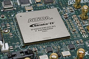
    English: Altera Stratix IV EP4SGX230 FPGA on a PCB
    Image via Wikipedia

    My supercomputer can beat your supercomputer, and money is no object. FPGAs (Field Programmable Gate Arrays) are used most often in prototyping new computer processors. You can design a chip, then ‘program’ the FPGA to match the circuit design so that it can be verified. Verification is the process by which you do exhaustive tests on the logic and circuits to see if you’ve left anything out or didn’t get the timing right for the circuits that may run at different speeds within the chip itself. They are expensive niche products that chip design outfits and occasionally product manufacturers use to solve problems. Less often they might be used in data network gear to help classify and reroute packets in a data center and optimize performance over time.

    This by itself would be a pretty good roster of applications, but something near and dear to my heart is the use of FPGAs as a kind of reconfigurable processor. I am certain one day we will see the application of FPGA  in desktop computers. But until then, we’ll have to settle for using FPGAs as special purpose application accelerators in high volume trading and Wall Street type data centers. This article in WSJ is going to change a few opinions about the application of FPGAs for real computing tasks. The speedups quoted for different analysis and reports derived from the transactions show multiple orders of magnitude speedups. In extreme examples sometimes 1,000 times faster speed-ups occurred when using a fully optimized FPGA versus a general purpose CPU.

    When someone can tout 1,000X speedups everyone is going to take notice. And hopefully it won’t be simply a bunch of copycats trying to speed up their reports and management dashboards. There’s a renaissance out there waiting to happen with FPGAs and I still have hope I’ll see it in my lifetime.

  • Xen hypervisor ported to ARM chips • The Register

    Deutsch: Offizielles Logo der ARM-Prozessorarc...
    Image via Wikipedia

    You can bet that if ARM servers suddenly look like they will be taking off that Red Hat and Canonical will kick in some help and move these Xen and KVM projects along. Server maker HP, which has launched the “Redstone” experimental server line using Calxedas new quad-core EnergyCore ARM chips, might also help out. Dell has been playing around with ARM servers, too, and might help with the hypervisor efforts as well.

    via Xen hypervisor ported to ARM chips • The Register.

    This is an interesting note, some open source Hypervisor projects are popping up now that the ARM Cortex A15 has been announced and some manufacturers are doling out development boards. What it means longer term is hard to say other than it will potentially be a boon to manufacturers using the ARM15 in massively parallel boxes like Calxeda. Or who are trying to ‘roll their own’ ARM based server farms and want to have the flexibility of virtual machines running under a hypervisor environment. However, the argument remains, “Why use virtual servers on massively parallel cpu architectures when a  1:1 cpu core to app ratio is more often preferred?”

    However, I would say old habits of application and hardware consolidation die hard and virtualization is going to be expected because that’s what ‘everyone’ does in their data centers these days. So knowing that a hypervisor is available will help foster some more hardware sales of what will most likely be a niche products for very specific workloads (ie. Calxeda, Qanta SM-2, SeaMicro). And who knows maybe this will foster more manufacturers or even giant data center owners (like Apple, Facebook and Google) to attempt experiments of rolling their own ARM15 environments knowing there’s a ready made hypervisor out there that they can compile on the new ARM chip.

    However, I think all eyes are really still going to be on the next generation ARM version 8 with the full 64bit memory and instruction set. Toolsets nowadays are developed in house by a lot of the datacenters and the dominant instruction set is Intel x64 (IA64) which means the migration to 64bits has already happened. Going back to 32bits just to gain the advantage of the lower power ARM architecture is far to costly for most. Whereas porting from IA64 to 64bit ARM architecture is something more datacenters might be willing to do if the potential cost/benefit ratio is high enough to cross-compile and debug. So legacy management software toolsets are really going to drive a lot of testing and adoption decisions by data centers looking at their workloads and seeing if ARM cpus fit their longer term goals of saving money by using less power.