My short 2009 review1 of Stewart Brand’s Whole Earth Discipline includes this Kevin Kelly quote that continues to resonate for me:
Kevin Kelly calls the book “a short course on how to change your mind intelligently” — in this case, about cities, nuclear power, and genetic and planetary engineering. These are all things that Steward Brand once regarded with suspicion but now sees as crucial tools for a sustainable world.
In Changeable minds I wrote about a touchstone question that I now sometimes ask people:
What’s something you believed deeply, for a long time, and then changed your mind about?
It’s a hard question for any of us to answer, but as Dave Gray and Wael Ghonim have recently reminded me, it matters more and more that we try. Here’s a useful picture I grabbed from Gray’s screencast on what he calls liminal thinking:
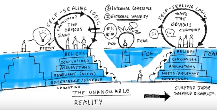
The idea is that…


